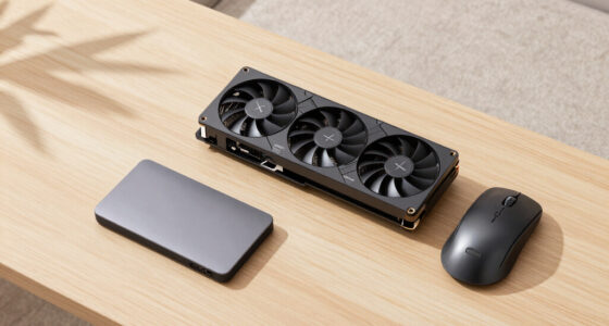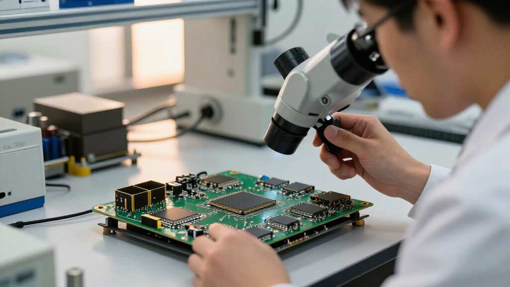
🔍 Read the full analysis: How An AI Chip’s Dies And HBM Stacks Work As A System on ThorstenMeyerAI.com

Get everyday essentials delivered free with Prime
- Fast, free delivery on millions of items
- Prime Video, Amazon Music and more included
- Member-only deals all year
TL;DR
ThorstenMeyerAI.com published a layer-by-layer explainer of how AI accelerator compute dies, high-bandwidth memory (HBM), silicon interposers and cooling operate as a package and rack system. The article reports that memory bandwidth and advanced packaging can constrain performance and supply, while specifications and production forecasts cited in the explainer come from chipmakers and other industry sources.
ThorstenMeyerAI.com published a hardware explainer on November 22 showing how AI accelerator compute dies, stacked high-bandwidth memory (HBM), silicon interposers and liquid cooling work together inside a package and across a rack. The report argues that memory bandwidth and advanced packaging, as well as compute capacity, can limit how quickly AI systems run and how many accelerators manufacturers can deliver.
The explainer describes an accelerator not as a single chip but as a collection of components. A package substrate connects the package to its module, while a silicon interposer carries dense wiring between compute dies and nearby HBM stacks. The memory towers contain DRAM chips joined vertically by through-silicon vias, or TSVs. A cold plate above the package carries liquid cooling.
For examples, the article cites Nvidia specifications describing the Rubin GPU as having two reticle-limited compute dies and 336 billion transistors. It says AMD’s MI350 Series integrates eight vertically stacked accelerator complex dies and two I/O dies; the MI355X has 185 billion transistors and eight 12-high HBM stacks, according to the source material. These are distinct design approaches, not a single standard layout.
The article also zooms out to the rack. Nvidia’s GB200 and GB300 NVL72 configurations are described as having 72 GPUs and 36 CPUs, distributed across 18 compute trays, alongside NVLink switch trays, management switches and power shelves. Nvidia identifies 120 kW of cooling capacity for a GB200 NVL72 rack. The explainer says its 3D models show layer order and counts, but use schematic dimensions because manufacturers do not publish the dimensions needed to establish exact package and stack sizes.
Why Memory and Packaging Matter
The package design shapes how much data can move between memory and compute. As AI models and workloads grow, fast processors need a steady flow of data; a compute die cannot deliver its potential if memory bandwidth or connections become a constraint. The article cites a rise in Nvidia GPU memory bandwidth from 900 GB/s for V100 to 19.2 TB/s for Rubin, figures taken from Nvidia product information. They describe different products and do not by themselves establish how a particular workload will perform.
Packaging also affects how many systems can be made. Silicon interposers and HBM stacks require specialized manufacturing, and the explainer identifies this assembly as a potential production bottleneck. It quotes SK hynix’s expectation that HBM demand will exceed supply through 2030; that is the company’s forecast, not a guaranteed outcome. For buyers, limits on memory and packaging capacity could constrain accelerator availability and influence prices, though the article does not quantify future costs.
At rack scale, these components bring power and cooling requirements into the same calculation as chip performance. A 72-GPU system is not simply 72 independent cards: its trays, interconnects, power delivery and liquid cooling must operate together. That matters to organizations planning AI infrastructure because component specifications alone do not describe the capacity or operating needs of a deployed system.
Products Worth Considering

Bose QuietComfort Ultra Headphones Gen 1, Lunar Blue

Samsung Odyssey G55C 32-Inch QHD Curved Gaming Monitor

Apple iPad 11-inch (A16), 128GB, Wi-Fi, Silver
As an affiliate, we earn on qualifying purchases.
From Silicon Dies to HBM Towers
The article’s account starts at the bottom of the package, with a miniature multilayer substrate that routes power and signals. Above it, an interposer connects the dies and HBM through many fine wires. TSMC describes its CoWoS-S packaging as using a large silicon interposer to accommodate logic dies and HBM cubes. The explainer says the company gives a capacity of up to 3.3 reticle areas, or about 2,700 mm², for that interposer approach.
A reticle is the maximum area a lithography scanner prints in one exposure. For larger packages, the article describes CoWoS-L as using silicon bridges embedded in a carrier layer. It reports that TSMC’s chief executive said on October 15, 2026, that the company was in production at five times reticle size and working toward larger designs. Those statements concern packaging capacity and development, rather than the dimensions of every product.
HBM stacks place DRAM layers over a base die and connect them vertically using TSVs. The article cites JEDEC’s April 2025 HBM4 standard, which allows stacks of four, eight, 12 or 16 layers and up to 64 GB per stack. It also cites manufacturer reports about thinner DRAM layers and tighter spacing. Such figures describe particular products or standards; they should not be read as proof that every accelerator uses the same stack height or memory capacity.
Limits of the Published Specifications
The source says its 3D models use schematic sizes because Nvidia and AMD do not publish exact dimensions for the dies, packages and memory stacks discussed. The models can illustrate component order and counts, but they do not establish physical scale. Product configurations and claims cited in the article also come from manufacturers and standards bodies; the explainer does not independently test performance or verify supply forecasts.
It is not clear from the source how much packaging capacity will be available to each chipmaker, how HBM supply will develop against demand, or how those factors will affect prices and delivery schedules. Nor do the cited bandwidth figures predict performance across different AI workloads. Actual results depend on the full system and software, not memory bandwidth alone.
Capacity and Rack Designs Ahead
The developments to watch are the rollout of newer accelerator packages, the availability of taller HBM stacks, and manufacturers’ ability to expand advanced packaging. The source reports TSMC is working on interposers larger than its stated five-reticle production scale, while SK hynix expects HBM demand to outstrip supply through 2030. Those are company statements and forecasts; delivery volumes and timing remain subject to change.
For deployed systems, the next practical milestone is whether rack-scale products can be supplied with the memory, power and liquid-cooling capacity their configurations require. The article lists Nvidia’s Vera Rubin NVL72 as available on the company’s site with 72 Rubin GPUs and 36 Vera CPUs. Availability listings can change, and the source does not provide independent sales or shipment data. Buyers will need current vendor specifications and delivery information to assess specific systems.
Key Questions
What is HBM in an AI accelerator?
High-bandwidth memory (HBM) is DRAM arranged in vertical stacks beside compute dies. Through-silicon vias connect the layers so data can move through the stack.
What does the silicon interposer do?
The interposer is a thin silicon wiring layer that connects compute dies and HBM stacks with dense connections. It sits above the package substrate.
Why can packaging limit AI accelerator supply?
Advanced packages require specialized interposers, memory stacks and assembly capacity. The article identifies packaging as a potential bottleneck, but does not quantify how much it constrains production.
How many GPUs are in an Nvidia NVL72 rack?
The GB200 and GB300 NVL72 configurations described in the source contain 72 GPUs and 36 CPUs, along with compute trays, NVLink switch trays, management switches and power shelves.
Are the article’s 3D models exact scale?
No. The source says the models show layer order and component counts but use schematic dimensions, because the manufacturers do not publish all the physical measurements needed for exact-scale models.
Source: ThorstenMeyerAI.com